Guide to Qualifying New Suppliers in Malaysia for Manufacturing Success
Malaysia is a premier manufacturing hub in Southeast Asia. According to the Malaysian Investment Development Authority (MIDA), “Malaysia, with its extensive trade....
By AMREP | Posted on August 22, 2025
In the world of electronics manufacturing, the quality of solder joints can make or break the performance of a product. A tiny imperfection in a solder connection might not seem like a big deal during production, but in real-world use, it can lead to malfunctions, short circuits, or complete device failure.
Whether you're building high-end PCBs for aerospace systems or consumer gadgets, understanding and preventing soldering defects is essential for delivering reliable products.
This blog will walk you through the most common soldering defects, their root causes, proven prevention strategies, and the inspection methods top manufacturers use to maintain quality.
Soldering defects occur when the connection between electronic components and the printed circuit board (PCB) is compromised. These flaws can happen during wave soldering, reflow soldering, or even manual soldering. Different soldering processes have different challenges:
Therefore, even a single defective joint can reduce product lifespan, trigger costly rework, and damage your brand reputation.
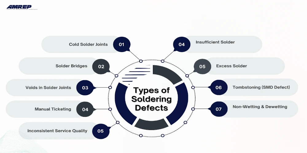
Cold solder joints have a dull, grainy, and uneven appearance, rather than the smooth, shiny look of a good connection. They typically occur when there isn't enough heat during soldering for the solder to flow and bond properly, or when contamination on the surfaces blocks good adhesion.
Risks and Consequences
Example: In a smartphone repair shop, a cold solder joint on a charging port caused the phone to charge only when the cable was held at a certain angle.
A solder bridge occurs when excess solder creates an unintended electrical connection between two pads or leads. It typically happens due to too much solder paste, poor stencil design, or misaligned components during placement.
Risks and Consequences
Example: A game console PCB failed right after assembly due to a solder bridge between two pins of a GPU, causing a complete power short.
Voids are small air or flux gas pockets trapped inside a solder joint when gases fail to escape before the solder solidifies. While some voiding is acceptable, large or frequent voids compromise joint quality.
Risks and Consequences
Example: In an automotive ECU, voiding in BGA joints caused overheating in power transistors, leading to engine stalling in hot climates.
When too little solder is applied, there isn't enough material to form a strong bond between the pad and component lead. It often results from clogged stencil apertures, poor paste transfer, or improper manual soldering.
Risks and Consequences
Example: A smartwatch assembly failed drop tests because insufficient solder on its battery connector caused intermittent power loss.
Applying more solder than needed may look secure, but it can overflow onto nearby pads or leads, creating unwanted connections and stress points.
Risks and Consequences
Example: In a power supply board, excess solder formed a blob that eventually touched a heatsink, creating an unexpected ground short.
Tombstoning happens when one side of a small surface-mount component lifts during reflow because of uneven heating. The imbalance in surface tension pulls the component upright, breaking one side's connection.
Risks and Consequences
Example: A Wi-Fi router failed RF testing because a tombstoned resistor in the antenna circuit cut off the signal path.
Non-wetting occurs when solder fails to spread across the pad at all, while dewetting happens when solder initially wets the pad but then retracts, leaving exposed areas. Both are signs of poor solderability.
Risks and Consequences
Example: In a medical device PCB, dewetting on sensor pads led to unstable readings, forcing the manufacturer to recall the batch.
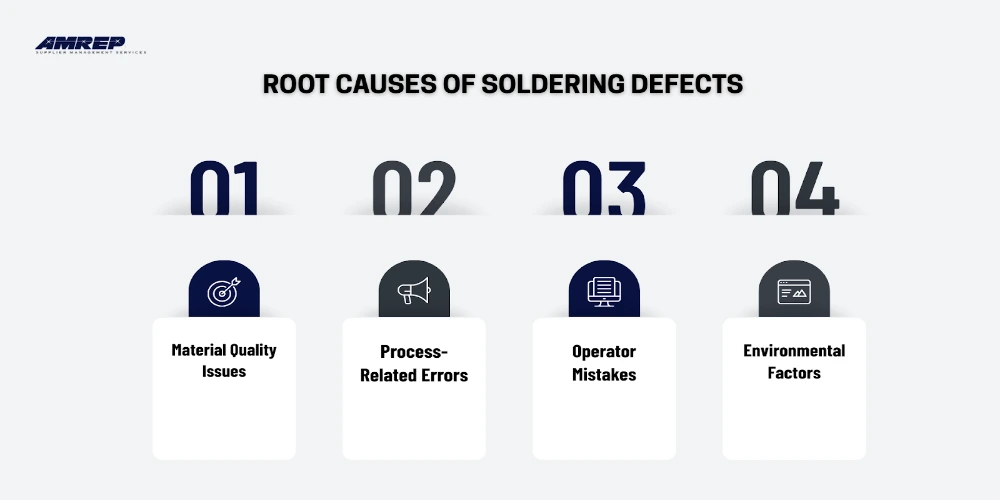
The quality of materials used in soldering directly impacts joint reliability.
Even high-quality materials can fail if the soldering process is poorly managed.
Human errors are a common cause of soldering defects, especially in manual soldering.
The production environment plays a significant role in soldering quality.
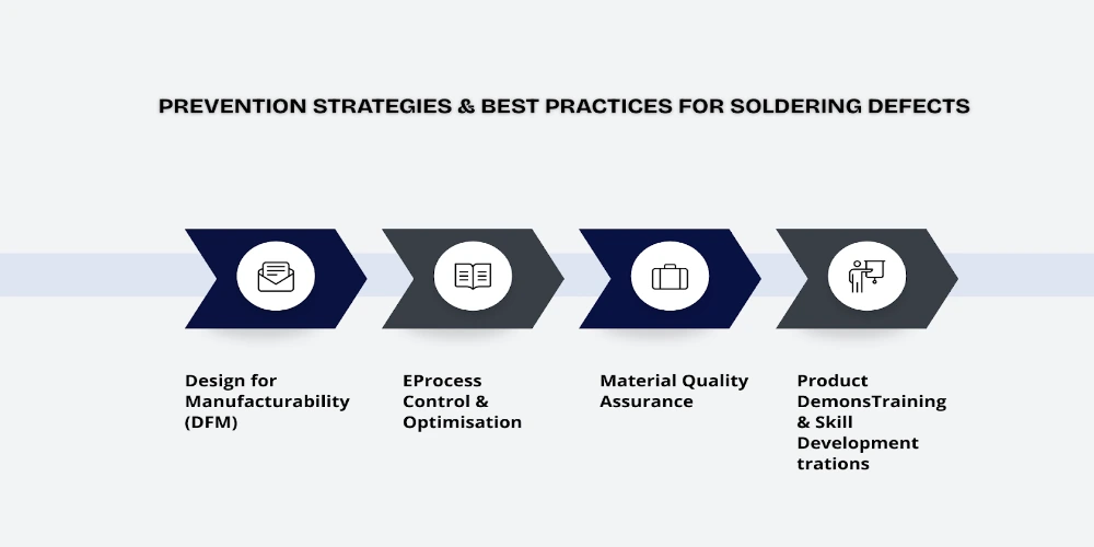
Good design is the first step toward preventing soldering defects. Ensuring that the PCB layout and component footprint follow industry standards can significantly reduce issues like bridging, tombstoning, or insufficient solder.
A well-controlled production process ensures that even high-volume manufacturing maintains consistent solder quality. Regular checks and adjustments help prevent temperature inconsistencies, paste misapplication, and contamination.
Using reliable, high-quality materials minimises the risk of defects from the start. Low-quality paste, flux, or PCB finishes can directly lead to poor wetting, voiding, or other soldering issues.
Even the best materials and processes won't succeed without skilled operators. Continuous training ensures staff stay updated with the latest soldering standards and techniques.
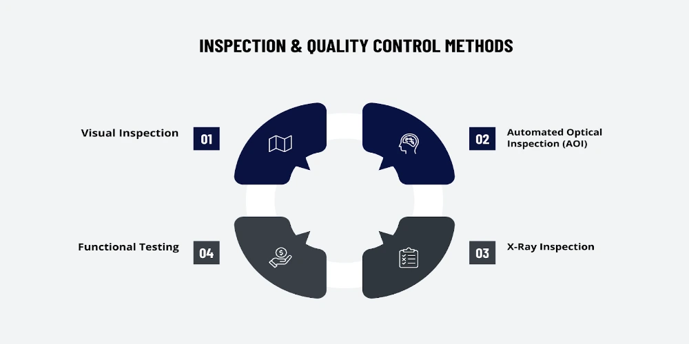
The most basic form of quality control is visual inspection, which allows technicians to quickly detect obvious soldering defects such as cold joints, excess solder, or misaligned components. It's often performed with magnifying lamps or microscopes for greater accuracy.
Key Features:
AOI uses high-resolution cameras and image-processing software to scan PCBs and compare them to a reference design. It can quickly detect solder bridges, missing components, incorrect orientations, and other defects.
Key Features:
X-ray inspection is essential for examining solder joints hidden beneath components like BGA (Ball Grid Array) or QFN packages. It reveals voids, insufficient solder, and other defects not visible from the surface.
Key Features:
Functional testing ensures the final product works as intended before it leaves the factory. It involves powering up the PCB and verifying its performance under simulated operating conditions.
Key Features:
Adhering to recognised industry standards, such as initial production inspections (IP), ensures that soldering quality is consistent, reliable, and in line with global best practices. These standards outline the acceptable levels of artistry, defect limits, and testing requirements for electronic assemblies.
The most widely used standard in electronics manufacturing is IPC-A-610. It defines the visual criteria for acceptable solder joints, component placement, cleanliness, and other quality parameters. Recognized globally, it serves as a benchmark for quality and consistency.
The standard that focuses on the process requirements for creating high-quality solder joints is IPC J-STD-001. It includes guidance on materials, methods, equipment, and verification procedures.
Following these standards ensures consistent manufacturing quality, enhances reliability and customer trust, and meets compliance requirements for industries such as automotive, medical, and aerospace.
Soldering defects may seem minor, but they can turn into costly repairs, delays, and brand damage. Fixing a defect during assembly might cost just $0.10, but if it's found in the field, that same issue can soar to $100+ per unit.
Ensure every product meets the highest standards—partner with AMREP’s inspection services and keep soldering defects out of your supply chain.
Electronics manufacturing is getting a big boost from new tech designed to spot and stop soldering problems before they become costly mistakes.
Soldering defects might seem small, but in electronics manufacturing, even the tiniest flaw can lead to big problems such as costly repairs, missed deadlines, and unhappy customers. Fortunately, most of these issues are preventable. By knowing what defects to look out for, tackling the root causes, and sticking to proven best practices, you can keep quality high and headaches low. And with today's AI inspection systems, smart reflow ovens, and better materials, it has become easier than ever to catch problems early and keep your products running flawlessly.
AMREP offers the best electronic quality engineering services and solutions to help manufacturers detect and prevent issues like cold joints, solder bridges, and other PCB assembly defects before they reach your customers.
Ready to elevate your quality control? Reach out and explore AMREP’s inspection services today.
Contact Us To See What We Can Do
Call Us
Mon - Sat 9.00 - 18.00
Sunday Closed


12 - May 2025
12
May
2025
Malaysia is a premier manufacturing hub in Southeast Asia. According to the Malaysian Investment Development Authority (MIDA), “Malaysia, with its extensive trade....

22 - April 2025
22
April
2025
Healthcare is rapidly evolving, ensuring consistent and high-quality patient care. Total Quality Management (TQM) in healthcare is more than just a buzzword—it is a powerful....

16 - April 2025
16
April
2025
Total Quality Management (TQM) is a mindset that involves everyone in the organization working toward a common goal: achieving excellence through quality. From....


Our website uses cookies to improve your experience. Read our Cookie Policy for more information.